
Blackwell vs. Rubin: NVIDIA's Next Generation Is Still a Leap — Just Not the One on the Poster
The comparison chart racing around LinkedIn uses NVIDIA's original Rubin numbers. In September, NVIDIA quietly lowered two of them. The gap over Blackwell is still wide — and the reason the numbers moved is the real story.
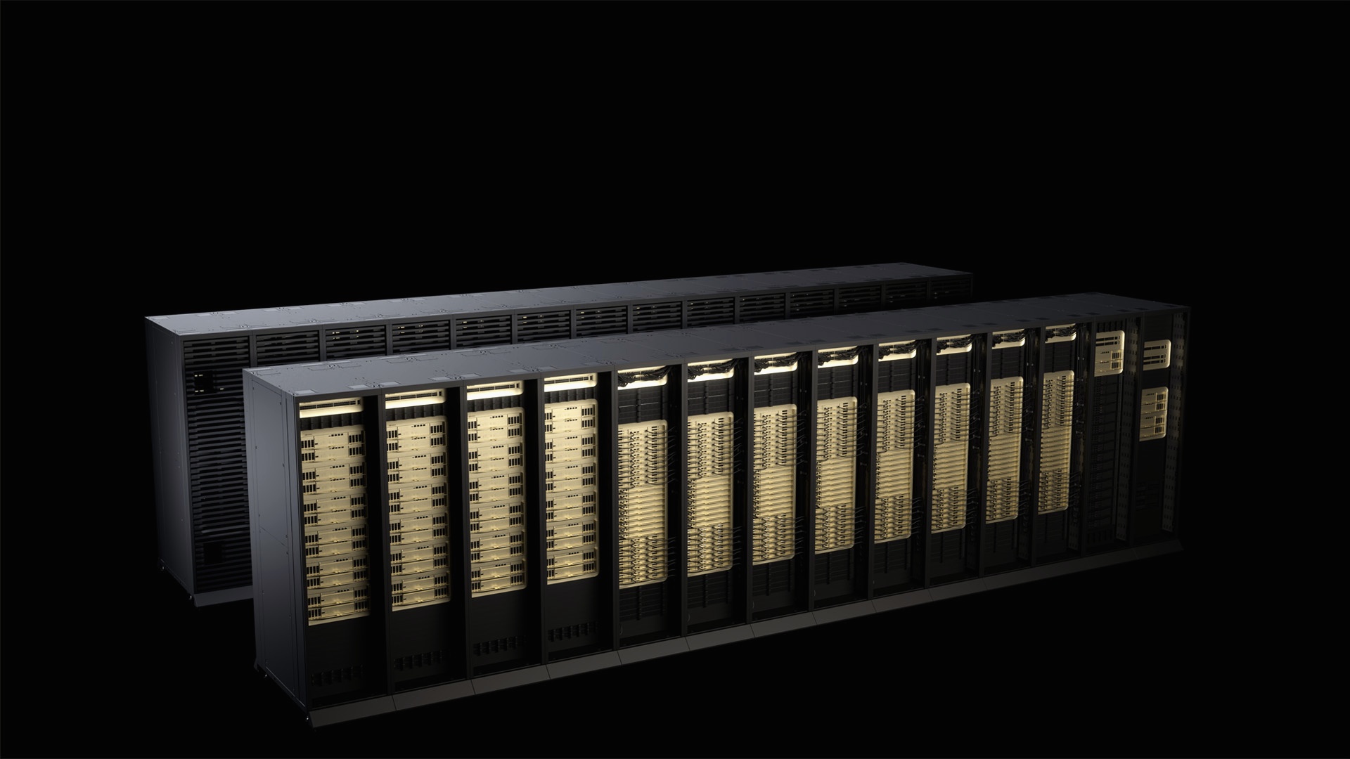
Photo: NVIDIA — Vera Rubin NVL72, official press image.
A clean, green-lit chart is making the rounds on LinkedIn: Blackwell on the left, Rubin on the right, and three rows of numbers that seem to settle the generational question in a single glance. Memory bandwidth jumps from 8 TB/s to 22 TB/s. NVLink doubles. Case closed.
Most of the chart checks out. But the two biggest Rubin numbers on it are no longer the numbers NVIDIA itself publishes — and the change happened without an announcement, a blog post, or a footnote anyone was meant to notice.
What the poster gets right
The Blackwell side of the comparison is accurate. The B200 carries 192 GB of HBM3e memory per GPU — 180 GB as exposed in NVIDIA's eight-GPU HGX boards — at 8 TB/s of bandwidth, with fifth-generation NVLink running at 1.8 TB/s per GPU. The B300, sold as Blackwell Ultra, raises capacity to 288 GB of HBM3e (270 GB in HGX form) and lifts dense NVFP4 compute to 15 petaFLOPS, while bandwidth and NVLink stay exactly where they were. Blackwell Ultra is a memory-and-compute refresh of the same silicon, not a new architecture, and it is the most powerful NVIDIA GPU shipping in volume today.
Rubin's headline, as announced, was bigger in every dimension. The Rubin GPU pairs two compute dies joined by NVIDIA's NV-HBI interface, 336 billion transistors in total, with 288 GB of HBM4 memory supplied across eight stacks. NVIDIA's published launch figures promised up to 22 TB/s of memory bandwidth — 2.75 times Blackwell's — and sixth-generation NVLink at 3.6 TB/s per GPU, double the Blackwell generation. Inference compute was rated at 50 PFLOPS of NVFP4. The Vera Rubin platform built around the chip was declared in full production at CES in January 2026, and NVIDIA said on May 31, 2026 that it was ramping into full production, with production shipments beginning in the fall of 2026.
The numbers that moved
Between September 1 and September 11, 2026, NVIDIA edited the Vera Rubin product pages. Archived snapshots of the pages, first flagged by ITHome and reported by TweakTown, show the per-GPU HBM4 bandwidth cut from 22 TB/s to 19.2 TB/s — a reduction of about 13 percent — and NVLink 6 bandwidth cut from 3.6 TB/s to 3.0 TB/s per GPU, about 17 percent. The rack-level figures moved with them: the Vera Rubin NVL72's aggregate HBM4 bandwidth now reads 1,400 TB/s, and the eight-GPU HGX Rubin NVL8, the configuration most cloud providers and enterprises will actually deploy, fell from 176 TB/s to roughly 130 TB/s of aggregate memory bandwidth.
Memory capacity did not change: 288 GB of HBM4 per GPU stands. Neither did the 50 PFLOPS NVFP4 inference figure. What changed is how fast data moves — and NVIDIA has not explained why. Reporting around the revision points to the HBM4 interface itself: a per-pin data rate reduced from 11.7 Gbps to 9.6 Gbps, possibly a consequence of NVIDIA's own bus design and signaling limits rather than the memory stacks, which are supplied by Micron, SK hynix, and Samsung. That explanation remains unconfirmed by NVIDIA.
Why bandwidth is the whole argument
The revision matters because memory bandwidth, not raw compute, is the constraint that decides how these machines perform in production. Large models spend much of their time waiting for weights and key-value data to arrive from memory; a GPU's FLOPS rating describes what it can do in the moments it is not waiting. This is why the B300's upgrade over the B200 was mostly memory, and why Rubin's advance over Blackwell was always going to be measured primarily in terabytes per second.
Measured that way, the generational step survives the correction. At 19.2 TB/s, a Rubin GPU still moves data 2.4 times faster than a Blackwell GPU's 8 TB/s. NVLink at 3.0 TB/s is still 1.67 times the 1.8 TB/s of the Blackwell generation, across a 72-GPU NVL72 fabric designed to behave as a single machine. The direction of the poster is right. The destination numbers are lower than printed.
The trim also redraws one line of the competitive map. With Rubin's published memory bandwidth reduced, TweakTown notes that AMD's Helios platform now leads on published memory bandwidth — a position that, on the original figures, was not available to it. Published specifications are not benchmark results, and delivered systems will settle the question. But vendors compete on the published page first, and that page changed.
What to watch
Blackwell and Blackwell Ultra remain the deployed mainstream: they are what the cloud instances, the DGX systems, and the enterprise orders are made of today. Rubin systems are only beginning to arrive, and the specifications that count will be the ones confirmed on delivered hardware, not the ones on any product page — original or revised.
The chart circulating this week is not wrong about where NVIDIA's AI infrastructure is going. It is wrong about how far along the numbers already are — because the numbers moved, quietly, in September, and almost nobody updated the poster.
𝐆𝐄𝐓 𝐅𝐑𝐄𝐄 𝐅𝐔𝐋𝐋 𝐌𝐀𝐆𝐀𝐙𝐈𝐍𝐄 𝐀𝐓 thebuyerspulse.com
Sources
- NVIDIA product pages and architecture materials for Vera Rubin and Blackwell Ultra (read November 16, 2026) — B200: 192 GB of HBM3e (180 GB in HGX boards) at 8 TB/s, NVLink 5 at 1.8 TB/s per GPU; B300 (Blackwell Ultra): 288 GB of HBM3e (270 GB in HGX), 15 PFLOPS dense NVFP4; Rubin as announced: 288 GB of HBM4, up to 22 TB/s, NVLink 6 at 3.6 TB/s per GPU, 336 billion transistors, dual-die NV-HBI, 50 PFLOPS NVFP4 inference.
- TweakTown, reporting on Wayback Machine captures of NVIDIA's Vera Rubin product pages dated September 1 and September 11, 2026 — the revision first flagged by ITHome: per-GPU HBM4 bandwidth cut from 22 to 19.2 TB/s; NVLink 6 cut from 3.6 to 3.0 TB/s per GPU; Vera Rubin NVL72 aggregate HBM4 bandwidth now 1,400 TB/s; HGX Rubin NVL8 from 176 to roughly 130 TB/s; reported HBM4 per-pin rate of 11.7 → 9.6 Gbps, unconfirmed by NVIDIA.
- NVIDIA statements: the Vera Rubin platform declared in full production at CES (January 2026); production ramp confirmed on May 31, 2026, with production shipments beginning in the fall of 2026.
- The comparison chart that motivates this story is by Farbod Alvandi (LinkedIn), with data attributed to NVIDIA; its image is not reproduced here.
- Photo: NVIDIA — Vera Rubin NVL72 systems, official press image published with NVIDIA's Vera Rubin platform technical blog (January 2026).